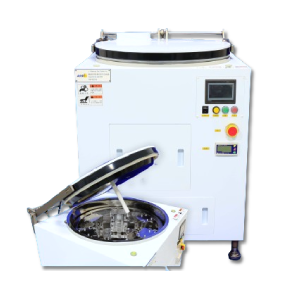
Plasma Clean, Photoresist Strip/Clean/Descum, HMDS Vapor Prime/Image Reversal, Silane Monolayer Deposition, Polyimide/BCB/PBO/Low Temp Polymer Cure, Self-Assembled Materials (SAM) Silane/HMDS Prime before PR, Polyimide/BCB/Other polymer cure, Wet Process