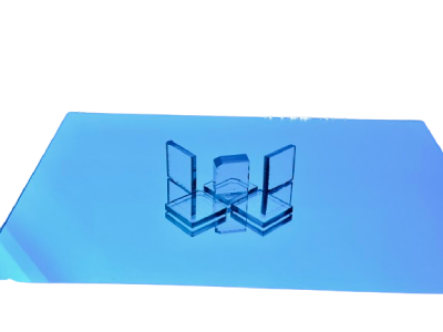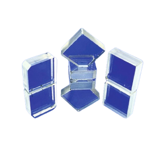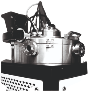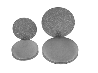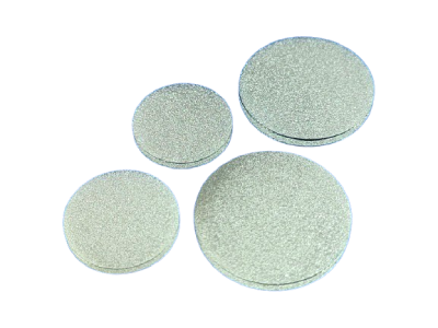
Ellipsometer, Laser Ellipsometer, Spectroscopic, Single Wavelength, Spectral photo luminsense Measurement, Deep Level Transient Spectroscopy (DLTS) Manual Measurement System (Non-destructive Fast, precise measurements of sheet conductance/ sheet resistance), The contactless, non-destructive alternative to Hall mobility, Measurement and Mapping Systems Contactless Bulk Resistivity/Sheet Resistance/ Capacitance Thickness.

Ellipsometer, Laser Ellipsometer, Spectroscopic, Single Wavelength, Spectral photo luminsense Measurement, Deep Level Transient Spectroscopy (DLTS) Manual Measurement System (Non-destructive Fast, precise measurements of sheet conductance/ sheet resistance), The contactless, non-destructive alternative to Hall mobility, Measurement and Mapping Systems Contactless Bulk Resistivity/Sheet Resistance/ Capacitance Thickness.

Nanolmprint Lithography (NIL) for R&D and production for LED/ OPTO, MEMS & NEMS, optical storage, Bio device, Magnetic storage display, semiconductor, polymer electronics and photovoltaic applications.

Nanolmprint Lithography (NIL) for R&D and production for LED/ OPTO, MEMS & NEMS, optical storage, Bio device, Magnetic storage display, semiconductor, polymer electronics and photovoltaic applications.

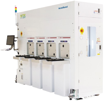
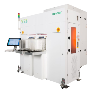
Coater & Developer tools – Semi-automated, Fully Automated (cassette-to-cassette coater developer) Microcluster tool – R&D and pilot production WET PROCESSING SYSTEMS Semi-automated, fully automated wet processing tools for cleaning, lift-off, etching and developing

Coater & Developer tools – Semi-automated, Fully Automated (cassette-to-cassette coater developer) Microcluster tool – R&D and pilot production WET PROCESSING SYSTEMS Semi-automated, fully automated wet processing tools for cleaning, lift-off, etching and developing

State of art dedicated standalone electron beam lithography systems – 50kVA series, 130kVA series Systems for R&D & for production too!

State of art dedicated standalone electron beam lithography systems – 50kVA series, 130kVA series Systems for R&D & for production too!
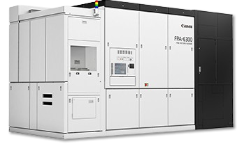
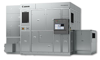
KrF Scanners / Steppers
i-line Steppers for Front-End-Of-the-Line (FEOL) Applications i-line Steppers for Back-End-Of-the-Line (BEOL) and Advanced Packaging Applications.


KrF Scanners / Steppers i-line Steppers for Front-End-Of-the-Line (FEOL) Applications i-line Steppers for Back-End-Of-the-Line (BEOL) and Advanced Packaging Applications.
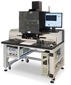
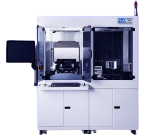
Mask Aligner, UV Exposure System, Solar simulator and Photovoltaic, UV meters
Mask Aligner ideal for Microelectronics, LED / HB LED, 3D IC, SIOP, WLP, 2.5D Interposer, MEMS, BioMEMS, MicroFluidics, Compound Semi, Solar (HCPV), and Optoelectronics applications.
MOCVD Systems, Gas and Vapor Delivery Control Systems, Wet Processing Technologies, Laser Annealing, Advanced Packaging Lithography, Deposition, Sputtering, Etch and Dicing/Lapping Systems MBE
Systems, Sources and Components, Atomic Layer Deposition Systems.

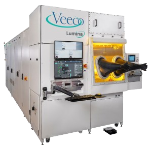
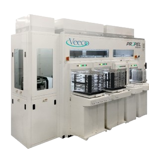
MOCVD Systems, Gas and Vapor Delivery Control Systems, Wet Processing Technologies, Laser Annealing, Advanced Packaging Lithography, Deposition, Sputtering, Etch and Dicing/Lapping Systems MBE
Systems, Sources and Components, Atomic Layer Deposition Systems.
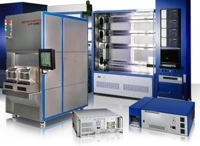

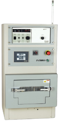
Thermco horizontal oxidation, diffusion furnace, Semithermo vertical diffusion furnace. Atmospheric, LPCVD process system.


Thermco horizontal oxidation, diffusion furnace, Semithermo vertical diffusion furnace. Atmospheric, LPCVD process system.
Electrochemical Capacitance-Voltage (ECV), Thin-film Stress Measurement Tool

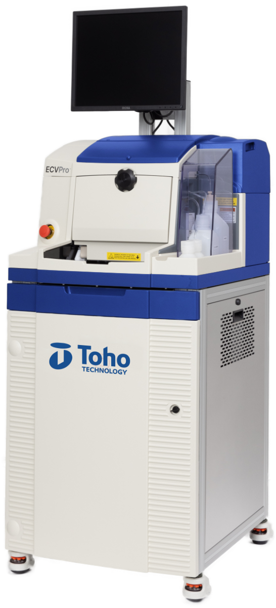
Electrochemical Capacitance-Voltage (ECV), Thin-film Stress Measurement Tool
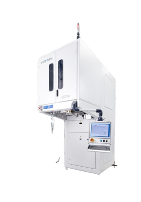
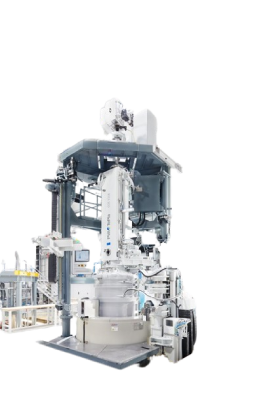
Cz-Systems – Czochralski (Cz) Method – Silicon, Germanium FZ-Systems- Floatzone (FZ) Method -Silicon SiCma Systems PVT Method – Silicon Carbide Kronos-Vertical Gradient Freeze (VGF) Method- Compound Materials


Cz-Systems – Czochralski (Cz) Method – Silicon, Germanium FZ-Systems- Floatzone (FZ) Method -Silicon SiCma Systems PVT Method – Silicon Carbide Kronos-Vertical Gradient Freeze (VGF) Method- Compound Materials
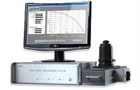
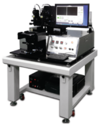

Hall Effect Measurement (HMS) system, Probe Station Prober, LED Tester, Rapid Thermal Processing System (RTP), Mask Aligner.

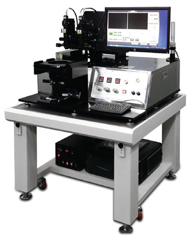
Hall Effect Measurement (HMS) system, Probe Station Prober, LED Tester, Rapid Thermal Processing System (RTP), Mask Aligner.
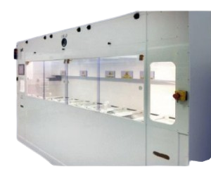

➢ T-Clean Wet Chemical Solutions
➢ Porous Silicon Formation
➢ Quartz Tube Cleaning Systems
➢ Semiconductor & Solar Wet Benches
➢ Semiconductor Cleaning Systems


➢ T-Clean Wet Chemical Solutions
➢ Porous Silicon Formation
➢ Quartz Tube Cleaning Systems
➢ Semiconductor & Solar Wet Benches
➢ Semiconductor Cleaning Systems
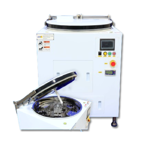
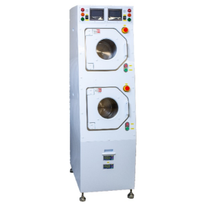

SRD (Spin, Rinse, & Dryer) – SV, Parts, Cassette


SRD (Spin, Rinse, & Dryer) – SV, Parts, Cassette
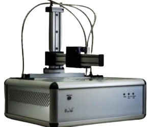

Non-destructive characterization of coatings in the Nano and micro-scale. Optical metrology tools for the characterization of single layer and multi-layer-coatings for a wide range of diverse applications. Film Characterization (thickness, optical properties), Absorbance, Fluorescence, Reflectance, Transmittance.


Non-destructive characterization of coatings in the Nano and micro-scale. Optical metrology tools for the characterization of single layer and multi-layer-coatings for a wide range of diverse applications. Film Characterization (thickness, optical properties), Absorbance, Fluorescence, Reflectance, Transmittance.
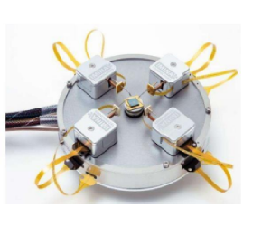

Modular robotic platforms are designed to fit all kind of scanning electron microscopes and optical setups. In situ nanoprobing and electrical failure analysis solutions for your SEM, FIB or dual beam Microprobing solutions for you


Modular robotic platforms are designed to fit all kind of scanning electron microscopes and optical setups. In situ nanoprobing and electrical failure analysis solutions for your SEM, FIB or dual beam Microprobing solutions for you
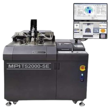
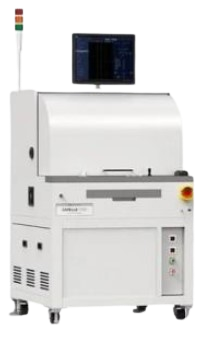
State of the art Probe Cards, Production LED Equipment, Advanced Semiconductor Test Equipments: Manual Probe station, Semi-Automatic, Automated, High Power probe station RF & MW.
Comprehensive portfolio of automated wafer/device test, measurement, and inspection solutions for Mini LED, Micro- LED, Laser Diode, Photodiode, LED and more.
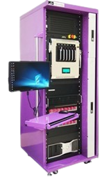
RF Reliability Burn-In System, HTOL / HAST Burn-In System, Automated Test Equipment (ATE), Yield Enhancement Metrology Tool, Parametric (WAT) Probe Card, Vertical Probe Card, MEMS VPC / CPC Probe Card,Test Socket & Contactor, Probe Station, μLED / VCSEL Integrated Test System, SiPH Test System, Power Device Analytical Tester, TMS / RMS / SPT Intelligent Test Operating System,Load board / Burn-In Board Substrates / PIB / PCI, WAT & Reliability Probe Card
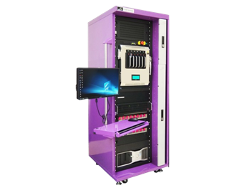
RF Reliability Burn-In System, HTOL / HAST Burn-In System, Automated Test Equipment (ATE), Yield Enhancement Metrology Tool, Parametric (WAT) Probe Card, Vertical Probe Card, MEMS VPC / CPC Probe Card,Test Socket & Contactor, Probe Station, μLED / VCSEL Integrated Test System, SiPH Test System, Power Device Analytical Tester, TMS / RMS / SPT Intelligent Test Operating System,Load board / Burn-In Board Substrates / PIB / PCI, WAT & Reliability Probe Card
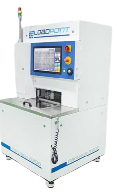
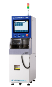

Dicing Solutions (6”, 8”, 12” dicing saw) Dicing Blades, Chucks Dicing and back griding tapes Mounting handling/blade dressing Dicing blade toc Automatic washing and drying station, Wafer mounter


Dicing Solutions (6”, 8”, 12” dicing saw) Dicing Blades, Chucks Dicing and back griding tapes Mounting handling/blade dressing Dicing blade toc Automatic washing and drying station, Wafer mounter
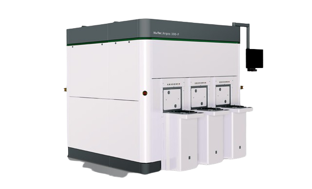
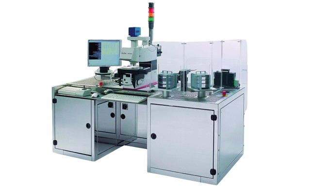
Defect Inspection for CD & Overlay Metrology:
CD Metrology
Overlay Metrology
Film Thickness


Defect Inspection for CD & Overlay Metrology:
CD Metrology
Overlay Metrology
Film Thickness
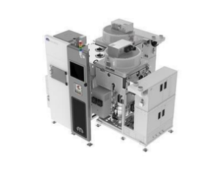

ICE Etcher , DRIE Etcher.CCP Etcher , LTD Etcher


ICE Etcher , DRIE Etcher.CCP Etcher , LTD Etcher

