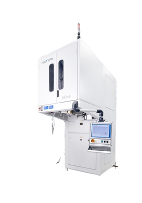
Thermco Horizontal Oxidation and Diffusion Furnace, Semithermo Vertical Diffusion Furnace: These systems support atmospheric and LPCVD processes. Complementing these are T-Clean Wet Chemical Solutions for applications such as porous silicon formation, quartz tube cleaning, and semiconductor/solar wet bench solutions, providing comprehensive semiconductor cleaning systems.
Inline Process Control:
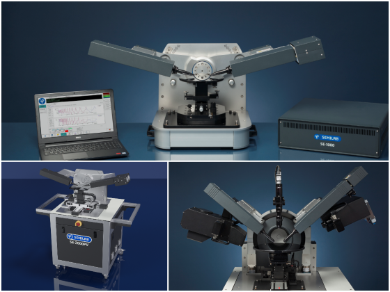
Carrier Lifetime (µ-PCD, QSS-µPCD)
Color Measurement for Cells
Photoluminescence Imaging
Sheet Resistance Measurement
Single-Wave Ellipsometry
Spectroscopic Ellipsometry
Thickness and Resistivity Measurement
Laboratory Applications:
Deep Level Transient Spectroscopy – PV
Light Beam Induced Current
Non-Contact C-V Profiling
Quasi Steady State – µPCD
Offline Process Control:
Carrier Lifetime (µ-PCD, QSS-µPCD)
Four Point Probe Sheet Resistance
Photoluminescence Imaging
Sheet Resistance Measurement
Single-Wave Ellipsometry
SI Ingot/Block Testing:
Blocks’ Photoluminescence Imaging
Bulk Resistivity Measurement
E-PCD Carrier Lifetime for Mono-Si
Infrared Block Imaging
P/N Type Determination
µ-PCD Carrier Lifetime for Multi-Si
SI Wafer Sorting
Geometry Inspection
Microcrack Inspection
Photoluminescence Imaging
Saw Mark Inspection
Surface-Contamination and Chipping Inspection
Thickness and Resistivity Measurement
µ-PCD Carrier Lifetime for Wafers
Thin Film Applications
Four Point Probe Sheet Resistance
Spectroscopic Ellipsometry (LTPS)
TCO Sheet Resistance
Visual Inspectio
Toho Technology
Thin film stress Measurement System, ECV Profiler
Ag Paste
Engineered for Modern Solar Technologies: Available in formulations tailored for TOPCon, HJT, and PERC cell architectures
Customizable Performance: Designed to meet varied electrical, adhesion, and printing requirements based on customer needs.
Reliable Manufacturing Standards: Produced in facilities operating under ISO 9001 and ISO 14001 compliant systems.
PVA TePla
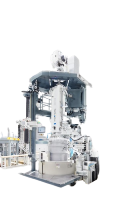
Floatzone (FZ) Method
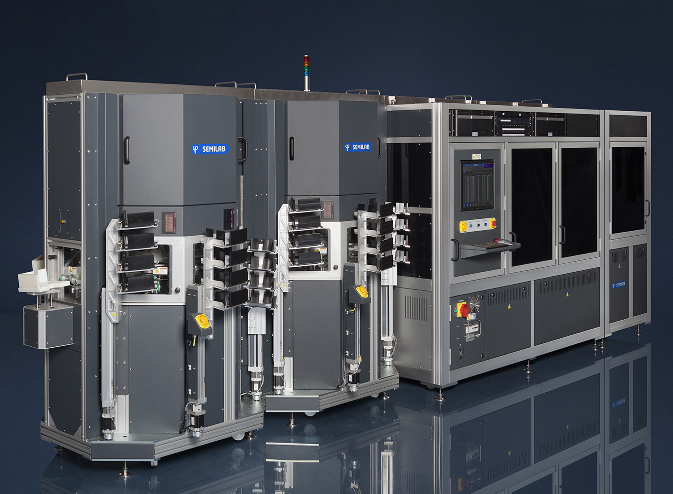
Thermco Systems
Thermco Horizontal Oxidation and Diffusion Furnace, Semithermo Vertical Diffusion Furnace: These systems support atmospheric and LPCVD processes. Complementing these are T-Clean Wet Chemical Solutions for applications such as porous silicon formation, quartz tube cleaning, and semiconductor/solar wet bench solutions, providing comprehensive semiconductor cleaning systems.
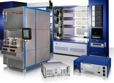
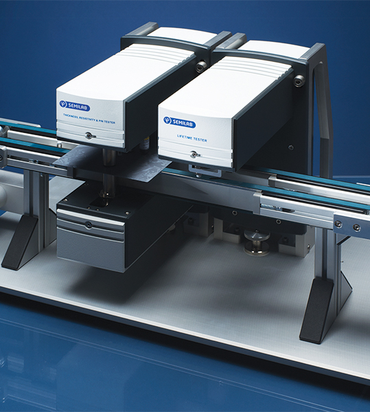
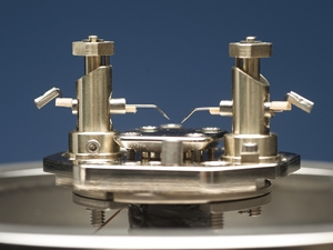
Semilab
Inline Process Control:
Carrier Lifetime (µ-PCD, QSS-µPCD)
Color Measurement for Cells
Photoluminescence Imaging
Sheet Resistance Measurement
Single-Wave Ellipsometry
Spectroscopic Ellipsometry
Thickness and Resistivity Measurement
Laboratory Applications:
Deep Level Transient Spectroscopy – PV
Light Beam Induced Current
Non-Contact C-V Profiling
Quasi Steady State – µPCD
Offline Process Control:
Carrier Lifetime (µ-PCD, QSS-µPCD)
Four Point Probe Sheet Resistance
Photoluminescence Imaging
Sheet Resistance Measurement
Single-Wave Ellipsometry
SI Ingot/Block Testing:
Blocks’ Photoluminescence Imaging
Bulk Resistivity Measurement
E-PCD Carrier Lifetime for Mono-Si
Infrared Block Imaging
P/N Type Determination
µ-PCD Carrier Lifetime for Multi-Si
SI Wafer Sorting:
Geometry Inspection
Microcrack Inspection
Photoluminescence Imaging
Saw Mark Inspection
Surface-Contamination and Chipping Inspection
Thickness and Resistivity Measurement
µ-PCD Carrier Lifetime for Wafers
Thin Film Applications:
Four Point Probe Sheet Resistance
Spectroscopic Ellipsometry (LTPS)
TCO Sheet Resistance
Visual Inspection
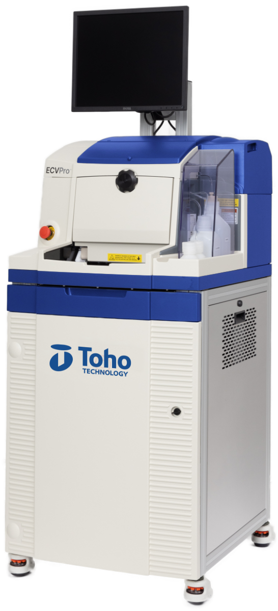
Toho Technology
Thin film stress Measurement System, ECV Profiler
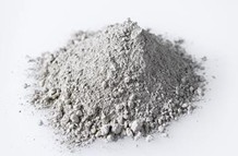
Ag Paste
Engineered for Modern Solar Technologies: Available in formulations tailored for TOPCon, HJT, and PERC cell
architecturesCustomizable Performance: Designed to meet varied electrical, adhesion, and printing requirements based on customer needs.
Reliable Manufacturing Standards: Produced in facilities operating under ISO 9001 and ISO 14001 compliant systems.