NANOTECHNOLOGY

NANOTECHNOLOGY

NT-MDT

Scanning Probe Microscope (AFM/STM/SNOM), Integrated SPM & Confocal Microscopy/Raman, Scattering Spectroscopy SPM, probes test samples, calibration, gratings. AFMRAMAN-SNOM, IR SNOM imaging, & spectroscopy, TERS.

ALEMNIS AG

In-situ nanoindentation technology for academic and industry. Compact, robust, versatile and can be fitted to various kinds of microscopes such as, Scanning Electron Microscopes (SEM), Light Microscopes, Synchrotron beamlines, and many more

Klocke Nanotechnik GmbH

Nanomanipulators For SEM, FIB, TEM. Lithography stage, Vacuum transfer system, vacuum gripper, Applications such as Manipulation, Nanocleaning, Nanoprobing, TEM-Lamella, 3D-nanofinger, Nanocutting, Force-distance, Partcile sorting, Nanofriction, Spot heater.

XENOS Semiconductor Technologies GmbH

E-Beam Lithography for SEM, FESEM & Dual Beam System. High speed pattern generators and other components for electron beam lithography, ion beam patterning fabrication and dual EB-FIB systems, beam blanker, stage.

Crestec Corporation

State of art dedicated stand alone electron beam lithography systems.

Obducat Technologies AB 

Nano Imprint Lithography (NIL) for R & D and production for LED/ OPTO, MEMS & NEMS, optical storage, Bio device, Magnetic storage display, semiconductor, polymer electronics and photovoltaic applications.

Semilab Co. Ltd.

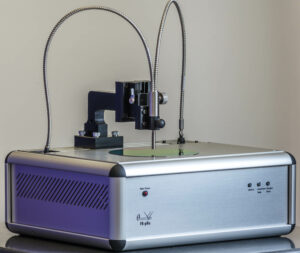
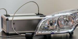
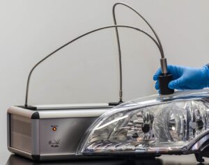
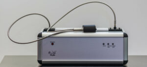
Spectroscopic Ellipsometry, Spectral Photoluminescence, Measurement, Mercury C-V Profiling, FTIR Reflectometry,  in-Situ Thickness Measurement , Roll To Roll Spectroscopic Elipsometery, Spectroscopic Reflectometer, Non-Contact C-V,Metrology, Non Contact Electrical Measurement, Stand Alone Nanoindentation System, Bulk Micro-Defect Micro Analyzer.

Graphene Square Inc.

CVD Systems for Graphene & 2D Materials, CVD Graphene Films, Graphene Oxide CVD, Graphene on TEM Grid, Graphene Quantum Dot and Accessories.

Theta Metrisis

FR-tools

Optical Metrology tools for the characterization of single layers and multi-layer coatings in the 1nanometer-1000micrometers thickness range and for a wide range of diverse applications, such as: semiconductors, organic electronics, polymers, paints and coatings, photovoltaics, biosensing.